The Key to Successful ESD Protection: GND Pattern Design and Use of ESD Protection Components

ESD Visualization System
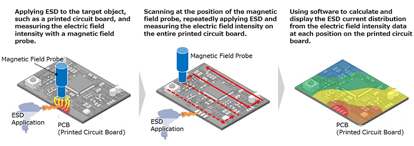
ESD visualization system enables the flow of ESD currents to be visualized by automatically scanning with a non-contact magnetic field probe (see Figure 1).
Evaluation Board for ESD Visualization Measurement
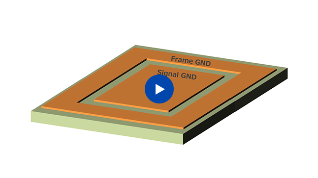
Front Side: A power-and-signal pattern is formed in the center of the board, and a Frame GND pattern around the perimeter.
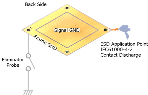
Back Side: A Signal GND pattern is formed in the center of the board, a 1mm gap between Signal GND and Frame GND patterns, and a Frame GND pattern around the perimeter (see Figure 2).
ESD Visualization Measurement Conditions
ESD Test Conditions: ESD is applied to the corner of the back side of the board. The eliminator probe is connected to the corner of the board placed diagonally to the ESD application point (see Figure 3).
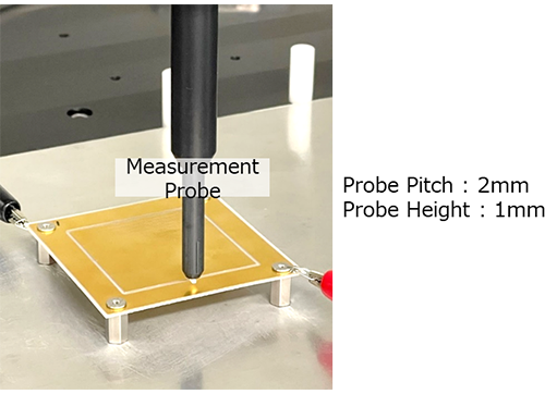
ESD Visualization Measurement Conditions: The measurement probe is set at the height of 1mm above the board surface and measures at 2mm intervals in the X and Y directions (see Figure 4).
Figure 3: ESD Test Conditions
Figure 4: ESD Visualization Measurement Conditions
Experiment 1: Confirming the Effect of the Gap between Frame GND and Signal GND Patterns (1)
Objective of the Experiment
When ESD is applied to the Frame GND pattern, we use the ESD visualization system to confirm whether the ESD current spreads to the Signal GND pattern, through a 1mm gap between Frame GND and Signal GND patterns.
Assumed Conditions
- Generally, ESD applied to a device intrudes from the outer edges of the board.
- Malfunctions of a device or IC due to ESD often occur when ESD intruding into the Signal GND disturbs the reference GND level.
- Since there is a 1mm gap between Frame GND and Signal GND patterns, ESD applied to the Frame GND pattern should not propagate to the Signal GND pattern. (The patterns are insulated from each other.)
- If the 1mm gap between the two patterns can prevent ESD from spreading from the Frame GND to the Signal GND pattern, this design can be used as PCB design with effective ESD countermeasure.
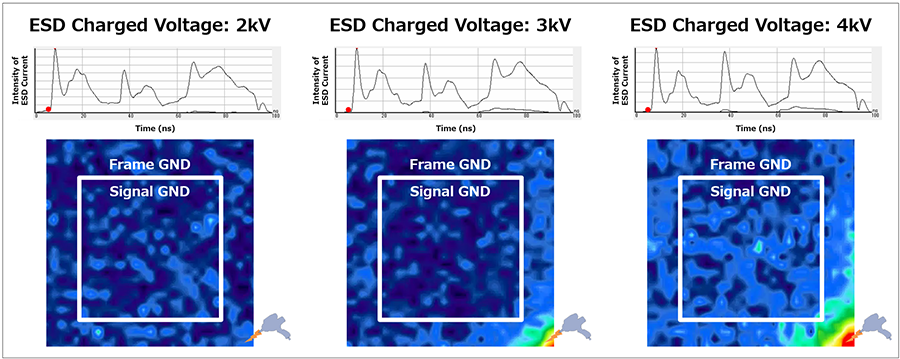
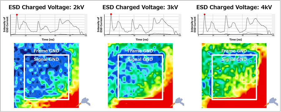
・No ESD intrusion to the Signal GND is observed.
・ESD current has entered the Signal GND pattern.
Summary of Experiment 1
- Although there is a 1mm gap between Frame GND and Signal GND patterns, ESD applied to the Frame GND pattern intrudes into the Signal GND pattern.
- The higher ESD charging voltage is, the more ESD current spreads from the Frame GND to the Signal GND pattern.
Experiment 2: Confirming the Effect of the Gap between Frame GND and Signal GND Patterns (2)
Objective of the Experiment
When a 5mm gap between Frame GND and Signal GND patterns is designed in consideration of the results of Experiment 1, we use the ESD visualization system to confirm whether the ESD current spreads to the Signal GND pattern.
Assumed Conditions
- The results of Experiment 1, shows that a 1mm gap between Frame GND and Signal GND patterns, allowed ESD applied to the Frame GND pattern to intrude into the Signal GND pattern.
- The gap of 1mm between Frame GND and Signal GND patterns is not sufficient to isolate ESD intruding from Frame GND from Signal GND pattern.
- When the gap between the patterns is increased to 5mm, Frame GND and Signal GND patterns are isolated from each other, which prevents ESD applied to the Frame GND pattern from propagating to the Signal GND pattern.
Summary of Experiment 2
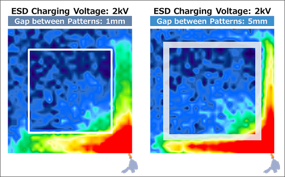
- There was no significant difference in ESD diffusion from Frame GND to the Signal GND pattern.
- Although there is a 5mm gap between Frame GND and Signal GND patterns, ESD applied to the Frame GND intrudes into the Signal GND pattern.
- It is challenging to prevent ESD from intruding from the Frame GND to the Signal GND pattern by just designing a gap between the patterns.
Why does ESD intrude the Signal GND pattern?
Depending on the strength of ESD and on the pattern shape, when ESD current flows to the Frame GND pattern, a magnetic field is generated around the pattern.
The generated magnetic field induces ESD current to propagate into the adjacent Signal GND pattern.
Experiment 3: Confirming the Effect of Components Mounted between Frame GND and Signal GND Patterns
Approach of Experiment 3
In Experiments 1 and 2, we considered measures to prevent ESD applied to the Frame GND pattern from intruding into the Signal GND pattern.
However, the results of Experiments 1 and 2 showed that introducing a gap between the patterns was insufficient to prevent ESD intrusion from the Frame GND to the Signal GND pattern.
In Experiment 3, we confirm whether ESD protection components can effectively divert ESD intruding into the Signal GND pattern, to minimize disruptions to the Signal GND reference level.
Objective of the Experiment
We use the ESD visualization system to confirm whether ESD protection components (chip varistors) can divert ESD current by mounting the chip varistors between Frame GND and Signal GND patterns.
Assumed Conditions
- The results of Experiments 1 and 2 shows that ESD applied to Frame GND pattern intrudes into Signal GND pattern.
- To prevent ESD from accumulating in the Signal GND pattern, we intentionally create a path for the ESD current to escape.
- If ESD can be directed from the Signal GND to the Frame GND pattern, this design can be used as PCB design with effective ESD countermeasure.
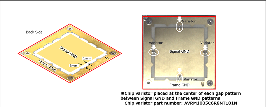
- An evaluation board with multiple protrusions inside the Frame GND pattern is used to mount chip varistors between Signal GND and Frame GND patterns.
- The gap between Signal GND and Frame GND patterns is narrowed to 1mm only at the chip varistors mounting position. (The gap is 3mm at other positions than for chip varistors mounting.)
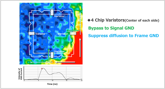
- Four chip varistors (L1.0 x W0.5mm, 6.8V) are placed mounted at the center of each gap pattern between Signal GND and Frame GND patterns.
ESD is bypassed to the Signal GND side by chip varistors which prevents spread of ESD to the Frame GND side.
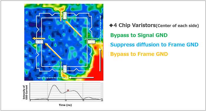
ESD bypassed to the Signal GND is then bypassed back to the Frame GND.
Summary of Experiment 3
- By mounting chip varistors between Frame GND and Signal GND patterns, ESD is bypassed to the Signal GND side via chip varistors.
- Furthermore, the ESD bypassed to the Signal GND is then bypassed back to the Frame GND through other chip varistors.
- The chip varistors functions as a pathway for ESD current to divert ESD intruding into the Signal GND to the Frame GND.
Summary
Those experiments aimed to confirm the effects of PCB GND pattern design to prevent ESD from intruding into the Signal GND for stabilizing the reference GND level. The following assumptions are based.
- Generally, ESD applied to a device intrudes from the outer edges of the board.
- Malfunctions of a device or IC due to ESD often occur when ESD intruding into the Signal GND disturbs the reference GND level.
In Experiments 1 and 2, we created a gap between Frame GND and Signal GND patterns to confirm the suppression effect on ESD intrusion from Frame GND to the Signal GND. The results showed that introducing a gap between the patterns was insufficient to prevent ESD intrusion from the Frame GND to the Signal GND pattern.
In Experiment 3, we explored the potential of diverting ESD that intrudes into the Signal GND back to the Frame GND instead of preventing ESD from intruding into the Signal GND.
The results showed that ESD is bypassed to the Signal GND side via chip varistors and then bypassed back to the Frame GND through other chip varistors.
It was found that mounting ESD protection components between the Frame GND and Signal GND functions as a pathway for ESD current to divert ESD intruding into the Signal GND.
By diverting ESD intruding into the Signal GND, it is possible to minimize disruptions to the Signal GND’s reference level and to function as a countermeasure against ESD-induced malfunctions in devices and ICs.
We believe that GND pattern design and utilization of ESD protection components will enable effective ESD countermeasures.
We hope the results of those experiments will contribute to designing circuits with high ESD robustness.
ESD Technical Support
TDK can conduct ESD tests compliant with IEC61000-4-2 and ISO10605 standards as well as can measure ESD suppression voltage waveforms.
Furthermore, we can measure ESD current using the ESD visualization system described in this article.
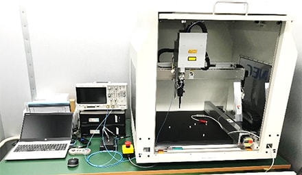
NEC Platforms, Ltd. - ESD Visualization System
- Features
- ◆ Can identify ESD paths.
- ◆ Can map ESD currents on the board.
- ◆ Can measure ESD in the nanosecond range.
- ◆ Can observe ESD behavior without being affected by the measurement system since non-contact measurement is possible.

