Flying Capacitors in PV Booster stages

The main advantages of switching between multiple voltage levels are lower voltage stress for the semiconductors and lower ripple stress for the power chokes.
This means that lower-voltage semiconductors can be used, which are typically cheaper.
Lower ripple stress for the chokes makes smaller and thereby lighter and cheaper choke designs possible.
The flying capacitor topology is a multilevel topology, that is an interesting choice especially for (but not limited to) the booster stage of a solar inverter. As its name implies, it needs a capacitor as a key element. This article describes and compares possible TDK solutions therefor.
Contents
Introduction
In a flying capacitor multi-level converter, additional (intermediate) voltage levels (beyond the two levels naturally given by the DC link) are generated using additional capacitors.
These capacitors can float to different electric potentials depending on the switching state of the semiconductor switching structure connected to them.
Therefore, they are called “flying capacitors”.
Once when charged to the right voltage (e.g. half the DC link voltage), they act as a kind of “voltage sources” for the duration of the next half switching cycle, thus providing additional voltage levels.
As these capacitors are exposed to high ripple currents and switching frequencies by this modus operandi while they must maintain a certain voltage,
it is important to carefully select the right components for this demanding application.
In the following, we will consider some design examples and component proposals for them.
Application conditions
The following assumptions apply: ΔUFC = 80 Vpp as the upper limit for the ripple voltage at the flying capacitor, a switching frequency of fSW = 16 kHz and a maximum peak current of Ipeak = 60 A. Therefore, the required capacitance of the flying capacitor is CFC = 24 µF, which can be calculated using the corresponding equation.
(Reference: Vincotech Technical paper "The Advantage and Operation of Flying-Capacitor Boosters")
The ambient temperature shall be 60 °C, assuming that the heat from the power modules does not significantly affect the flying capacitor. The generated heat is dissipated mainly through the PCB with a smaller fraction being dissipated into still air by natural convection.
Various capacitor technologies can be considered for this application. However, in the following the focus will be on TDK film capacitor and CeraLink® ceramic capacitor technology:
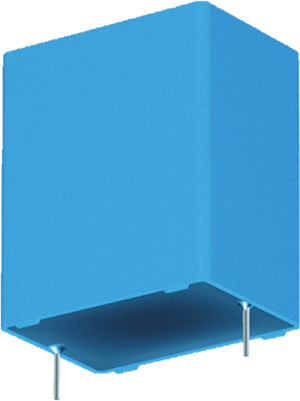
Film Capacitors for PCB Mounting
TDK offers different voltage and capacitance ranges for primary customer requirements in DC link operation. The mechanical design varies from 2 to 4 pins, while different lead space options also improve some electrical characteristics, such as low self-inductance and high resonance frequency. High resonance frequency, energy density, ripple current, ambient temperatures up to 125 °C and humidity protection are, in addition to long life expectancy (> 100k hours) and capacitance value stability, excellent design options for high-frequency switching applications.
For capacitor selection, modelling data and application simulation please check our CLARA (Capacitor Life And Rating Application) website.
CeraLink® Capacitors
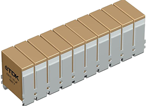
CeraLink® is a family of very compact capacitors for stabilizing voltages in the DC link or for use in snubber applications. These products are based on a unique antiferroelectric ceramic technology whose material exhibits increasing capacitance with increasing voltage. CeraLink® is designed to provide engineers with compact components, optimized for fast switching converters (e.g. SiC/GaN), converters with very tight space requirements and converters that must withstand high operating temperatures of up to 150 °C.
It is important to note that the capacitance behaviour of CeraLink® is non-linear and optimized for operation under DC-Bias and elevated ambient temperature, see our Technical Guide or our Simulation Toolbox for further details. With a DC-Bias level of 600 VDC and a super-imposed ripple voltage of 80 Vpp a CeraLink® FA10 700V type can be considered, offering an effective capacitance of typically 4 µF in the temperature range of 25-60 °C.
Comparison of Film Capacitors and CeraLink® Capacitors
The following tables compare the geometrical and electrical characteristics of the two considered capacitor solutions. If there are no space constraints, the film solution has more advantages in terms of cost and number of components, since one or a few parts can meet the electrical requirements. In contrast, CeraLink® could be an option if the total height of the solution is crucial or through-hole technology is not possible. Furthermore, CeraLink® shows clear advantages when a higher current capability is required and/or if the switching frequency is increased.
| Parameters | Unit | Film Capacitor (B32714H8805J000)** |
CeraLink Capacitor FA10 (B58035U7505M001) |
| Width (max) | [mm] | 18.0 | 7.8 |
| Height (max) | [mm] | 33.0 | 9.6 |
| Length (max) | [mm] | 31.5 | 30.5 |
| Volume | [cm³] | 18.7 | 2.3 |
| Landing pad width | [mm] | - | 10.7 |
| Landing pad length | [mm] | - | 31.0 |
| Footprint | [cm²] | 5.7 | 3.3 |
| Weight | [g] | 24.5 | 11.5 |
| Capacitance | [µF] | 8.0 | 4 |
| Capacitance per footprint | [µF/cm²] | 1.4 | 1.21 |
| Capacitance per volume | [µF/cm³] | 0.43 | 1.74 |
| Current capability | [ARMS] | 10.9 | 16.0 * |
| Rated Voltage | [Vdc] | 800 | 700 |
| Total number of required caps | [pcs] | 3 | 6 |
| Total footprint of solution | [cm²] | 17.1 | 19.8 |
| Total volume of solution | [cm³] | 56.1 | 13.8 |
| Total weight of solution | [g] | 73.5 | 69.0 |
| Total current capability | [ARMS] | 32.7 | 96 * |
Advantage
| Mounting technology | Through-hole | Surface mount |
* at 16kHz and 65°C ambient temperature, 150°C device temperature, no forced cooling.
** Configuration for an expected life endurance time > 88k hours in continuous application @65°C Ambient temp.
| Parameters | Unit | Film Capacitors (B32774H1335K000)** |
CeraLink Capacitor FA10 (B58035U7505M001) |
| Width (max) | [mm] | 19.0 | 7.8 |
| Height (max) | [mm] | 30.0 | 9.6 |
| Length (max) | [mm] | 31.5 | 30.5 |
| Volume | [cm³] | 17.9 | 2.3 |
| Landing pad width | [mm] | - | 10.7 |
| Landing pad length | [mm] | - | 31.0 |
| Footprint | [cm²] | 5.9 | 3.3 |
| Weight | [g] | 20.3 | 11.5 |
| Capacitance | [µF] | 3.3 | 4 |
| Capacitance per footprint | [µF/cm²] | 0.55 | 1.21 |
| Capacitance per volume | [µF/cm³] | 0.18 | 1.74 |
| Current capability | [ARMS] | 11.8 | 22 * |
| Rated Voltage | [Vdc] | 1100 | 700 |
| Total number of required caps | [pcs] | 4 | 3 |
| Total footprint of solution | [cm²] | 23.6 | 9.9 |
| Total volume of solution | [cm³] | 71.6 | 6.9 |
| Total weight of solution | [g] | 81.2 | 34.5 |
| Total current capability | [ARMS] | 47.2 | 66 * |
Advantage
| Mounting technology | Through-hole | Surface mount |
* at 32kHz and 65°C ambient temperature, 150°C device temperature, no forced cooling.
** Configuration for an expected life endurance time > 200k hours in continuous application @65°C Ambient temp.
Conclusion
The flying-capacitor booster is a high-efficient, low cost solution for solar inverter applications. The main advantages are the frequency multiplication, the lower semiconductor voltage, the lower voltage and current ripple, the lower switching losses, and the low EMI emission.
TDK has an extensive line-up of various capacitor technologies, which can support a wide range of capacitance and voltage values. Details can be viewed by clicking on the product types


