TLVR Inductors for Server Power Supply Circuits

In response to these market trends, semiconductor processors like CPU, GPU, FPGA, and others have made significant strides in their manufacturing process technology, with a notable focus on miniaturization. These advancements have led to increased gate integrations per unit area, higher operating frequencies, and substantial improvements in information processing capabilities.
In line with the improvement in processor capabilities, there have also been significant advancements in Server Power Circuits.
Table of Contents
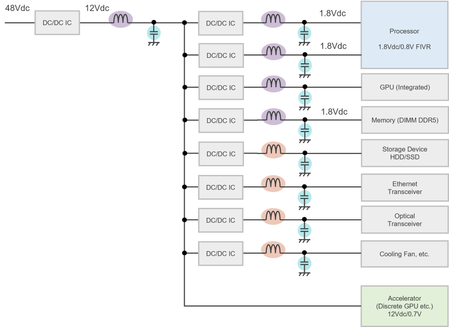
Current State of Server Power Supplies
As semiconductor processors continue to be smaller, their power supply voltages are decreasing. However, the increasing current consumption is causing a rise in overall power usage.
A problem that arises as we move towards low voltage and high current is the response to rapid load changes.
Due to the trend towards lower voltages, the tolerable voltage variation becomes extremely small. For instance, to avoid malfunctions in the processor, if the core voltage needs to be supplied with an accuracy of ±3%, then a voltage of 1V would require a tight control within ±30mV. In server power supplies, it is critical to maintain the output voltage as stable as possible, even under driving conditions that involve sudden, high-current loads exceeding 1,000A.
Previously, this move towards low-voltage and high-current scenarios could be handled by increasing the frequency (high-frequency operation) and adopting multi-phase regulation.
In multi-phase Voltage Regulator (VR) systems, it's not sufficient to control the duty cycle in a single phase to cope with large fluctuations in current. Multi-phase duty control is necessary.
However, switching between phases takes time, which necessitates even higher frequencies to improve response time.
High-frequency operation significantly improves load responsiveness, but it also results in considerable losses in switching components. This is problematic for server power supplies, where energy efficiency is a key feature, making it challenging to increase the frequency further in existing multi-phase VR configurations.
To mitigate the issue of large current fluctuations, using large external capacitors is an option, but it comes with increased footprint and cost concerns.
To address these challenges, a circuit configuration known as TLVR(Trans-Inductor Voltage Regulators) is now the mainstream approach for high-speed load fluctuation in low-voltage, high-current applications.
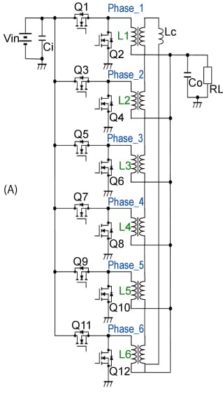
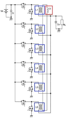
This configuration adds windings to the inductors connected to each phase switch. These are connected in a series loop with a compensating inductor for each phase, allowing simultaneous current supply from all phases. TLVR minimizes power losses while providing high transient response performance in semiconductor processors. It also allows for reducing the value of output capacitors, thereby cutting down on system costs and footprint.
TLVR Circuit Configuration
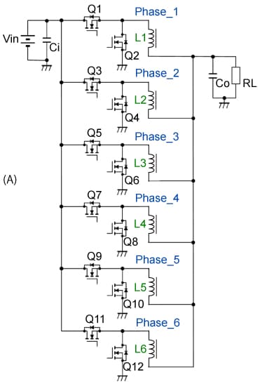
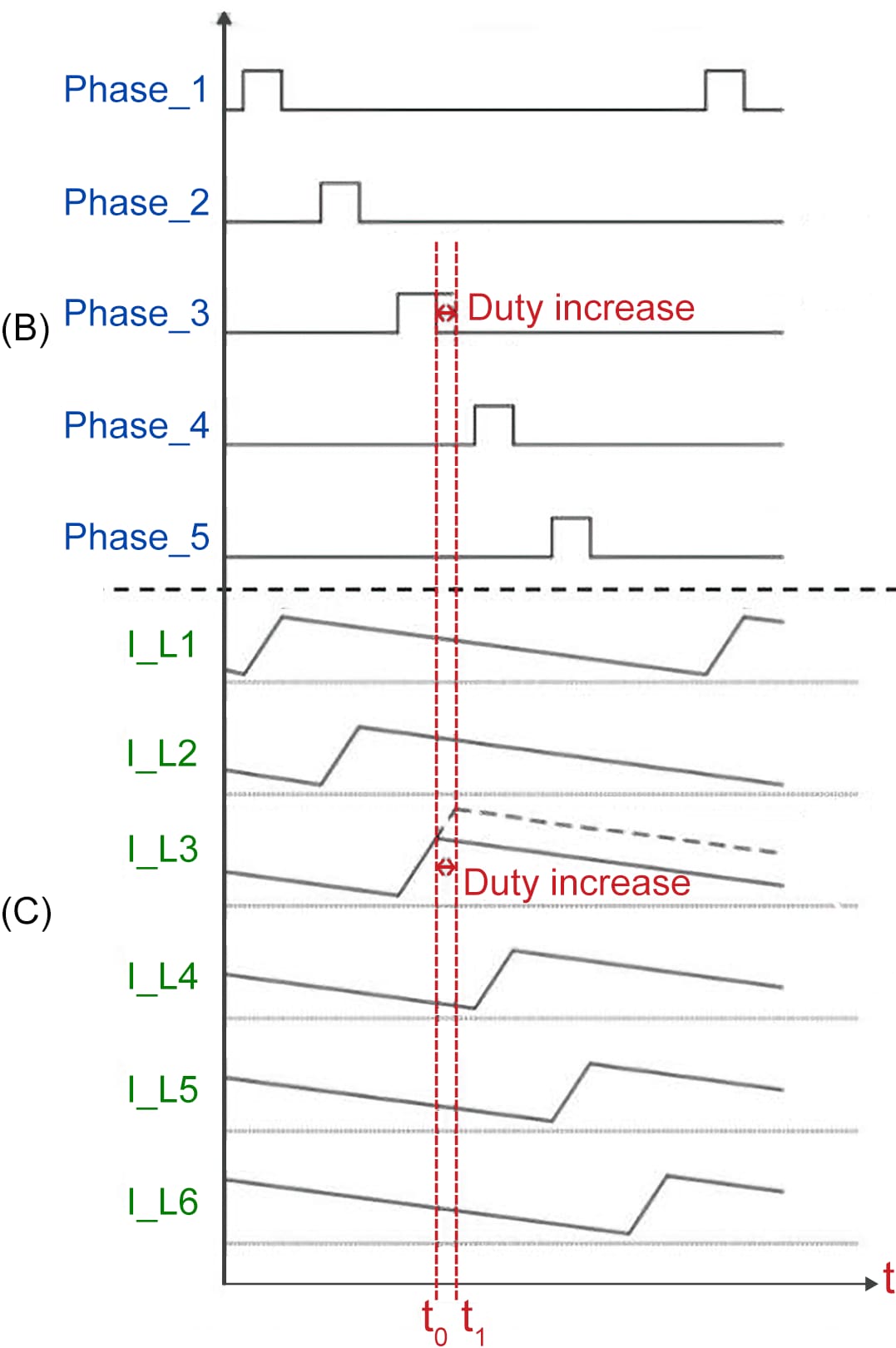
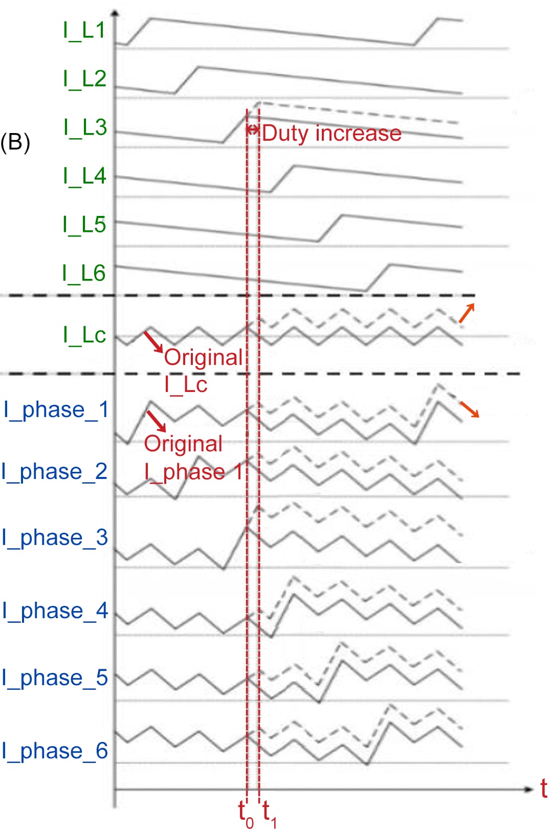
Figure 2 illustrates the operating mechanism of TLVR. When the current demand suddenly increases in a multi-phase VR, the duty cycle of the phase that is turned on at that timing expands to maintain the output voltage, thereby increasing the output current. By expanding the duty cycle of a specific phase, the output current of that phase can be increased. However, when a large current load fluctuation occurs, the current value is insufficient, and it responds to the increase in output current by expanding the duty of the following multiple phases.
In this case, the time it takes to secure the necessary current demand is unacceptably long, the slew rate of the output current is low, and it can't adequately respond to the rapidly changing load.
On the other hand, in TLVR, each phase switch is connected to an inductor with an added winding, and the added winding on each inductor is connected in a series loop with a compensating inductor. With this circuit configuration, when there is a sudden large increase in current demand, not only does the duty of the phase that is turned on at that timing expand to increase the output current, but it also works in conjunction with other inductors that are not turned on. It can supply current from all inductors at the same time. This allows for a high transient response to large current load fluctuations without significantly lowering the power supply voltage.
The TLVR method, which can supply current at high speed, is also effective in reducing the output capacitor and has become the mainstream circuit configuration today.
| Multi-phase VR | TLVR |
|---|---|
|
|
(C) (D) New I_Lc New |
| Fig: Operation of a traditional multi-phase voltage regulator. (A) Circuit Configuration (B) PWM waveforms that drive each phase (C) Voltage regulator response during a load transient |
Fig: Transient operation of a TLVR. (A) Circuit Configuration (B) Currents through the inductor of each phase (C) Current through the secondary winding (D) Output current of each phase |
Load Response Simulation Using TLVR
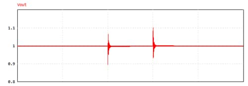
Under specific conditions, as a comparative example, we utilized a circuit simulator to compare the change in output voltage during sudden load changes between an 8-phase multi-phase VR and TLVR.
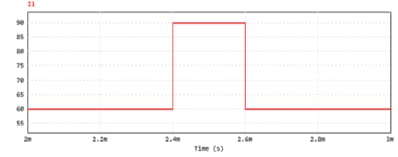
The following results were obtained assuming a switching frequency of 800kHz for a conversion from 12V to 1.8V and using an output smoothing capacitor value of 1,850μF for a load change of 240A→360A→240A.
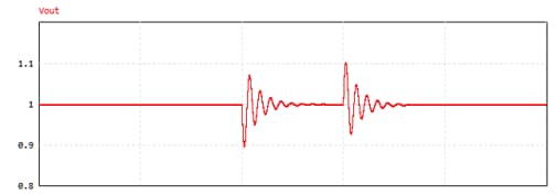
As a result, the load voltage fluctuation in the multi-phase VR was ±0.3V relative to 1.8V.
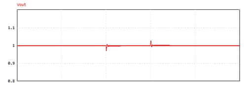
Meanwhile, the output fluctuation in TLVR was less than ±0.1V. We also confirmed that the time required for voltage stabilization could be significantly reduced with TLVR.
If we assume an acceptable voltage fluctuation of ±0.3V during load changes, by adopting the TLVR circuit configuration, the value of the output smoothing capacitor can be reduced to approximately 230μF, which is nearly 1/8th of its original size. This also confirmed that the time needed for voltage stabilization could be significantly shortened.
Multi-phase VR
TLVR
Expected drive conditions: Vin = 12V
Vo = 1.8V-240A, Fsw = 800kHz
Load variation: Io = 240A⇒360A⇒240A
Inductance value: L1-L8 = 120nH
Load variation
| Circuit Configuration | Voltage Fluctuations |
|---|---|
| Multi-phase VR C:1850μF |
|
| TLVR C:1850μF |
|
| TLVR C:230μF |
VLBUC Inductors Optimized for TLVR Circuit Configuration
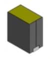
Introducing the dual coil power inductor VLBUC series and the LC compensation power inductor VLBU6565100, both of which have been optimized for the TLVR circuit configuration.
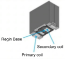
The VLBUC12060120 series is a dual coil power inductor that can handle large currents. It achieves low losses due to its high saturation magnetic flux density, optimization for high-frequency switching, a unique magnetic material, and a proprietary electrode structure. The inductor ensures a withstand voltage of DC100V between the two coils.
The VLBU6565100 series is specifically designed as an LC compensation power inductor. It prioritizes low losses in high-frequency bands.
Both series can operate within a temperature range of -40°C to +125°C.



For 6 Phases
Dual Coil Power Inductor – VLBUC Series
| TDK Identification | Coil | Inductance | Lk | K | Test | DC Resistance | Rated DC Current (A) | ||||
|---|---|---|---|---|---|---|---|---|---|---|---|
| at 0A (nH) |
Tol. (%) |
(nH) | (-) | Freq. (kHz) |
Spec.Typ (m-Ohm) |
Tol. (%) |
Isat_20% Typ. | Itemp_40C Typ. |
|||
| 25°C | 100°C | ||||||||||
| VLBUC12060120R08MF4 | Primary Secondry |
80 80 |
+/-20% +/-20% |
4.1 | 0.95 | 100 100 |
0.125 0.45 |
+/-10% +/-10% |
168 | 131 | 70 40 |
| VLBUC12060120R10LF4 | Primary Secondry |
100 100 |
+/-15% +/-15% |
4.1 | 0.96 | 100 100 |
0.125 0.45 |
+/-10% +/-10% |
132 | 104 | 70 40 |
| VLBUC12060120R12LF4 | Primary Secondry |
120 120 |
+/-15% +/-15% |
4.5 | 0.96 | 100 100 |
0.125 0.45 |
+/-10% +/-10% |
107 | 86 | 70 40 |
| VLBUC12060120R15LF4 | Primary Secondry |
150 150 |
+/-15% +/-15% |
4.5 | 0.97 | 100 100 |
0.125 0.45 |
+/-10% +/-10% |
89 | 71 | 70 40 |
| VLBUC12060120R17LF4 | Primary Secondry |
170 170 |
+/-15% +/-15% |
4.4 | 0.97 | 100 100 |
0.125 0.45 |
+/-10% +/-10% |
72 | 58 | 70 40 |
Note) Isat_20%: Depend on the Inductance Saturation when only supply DC current into Primary Coil.
(-20% Reduction from Initial L Value)
Itemp_40C: Depend on the Self Temperature Rise (40deg.C)
when only supply DC current into Primary Coil or Secondry Coil.
Lp(L primary): pin1-pin4
Lk(L leakage): pin1-pin2(When pin3 and pin4 are shorted)/2
K(Coupling factor) : 1-(Lk/Lp)
LC Compensation Power Inductor – VLBU6565100 Series
| TDK Identification | Inductance | Test | DC Resistance | Rated DC Current (A) | ||||||
|---|---|---|---|---|---|---|---|---|---|---|
| at 0A (nH) |
Tol. (%) |
Freq. (kHz) |
Spec.Typ (m-Ohm) |
Tol. (%) |
Isat_20% Typ. | Isat_30% Typ. | Itemp_40C Typ. |
|||
| 25°C | 100°C | 25°C | 100°C | |||||||
| VLBU6565100R10LF4 | 0.10 | +/-15% | 100 | 0.17 | +/-10% | 83 | 70 | 86 | 73 | 70 |
| VLBU6565100R12LF4 | 0.12 | +/-15% | 100 | 0.17 | +/-10% | 65 | 55 | 68 | 57 | 70 |
| VLBU6565100R15LF4 | 0.15 | +/-15% | 100 | 0.17 | +/-10% | 50 | 42 | 53 | 44 | 70 |
Note) Isat_20%: Depend on the Inductance Saturation. (-20% Reduction from Initial L Value)
Isat_30% : Depend on the Inductance Saturation. (-30% Reduction from Initial L Value)
Itemp_40C: Depend on the Self Temperature Rise (40deg.C)

