Audio line solution for smartphones using chip varistors - An overview
A TVS diode or chip varistor (multilayer chip varistor) is normally inserted into the audio lines of smartphones, namely the speaker line and head phone line, to suppress ESD (electrostatic discharge). But, to suppress noise in audio lines, ESD immunity alone is not enough, and electromagnetic noise emitted from the circuit wiring inside the smartphone must also be suppressed.
Chip varistors from TDK not only provide ESD suppression in audio lines, but are also ESD protection components which meet a variety of requirements specific to audio lines, such as the following:
- Significant reduction in mounting area
- Low audio distortion
- Improved noise sensitivity
- Noise suppression
TDK offers following chip varistors for audio line solutions
| For the headphone line | For the speaker line | ||
|---|---|---|---|
| AVRM0603 type | AVRM1005 type | ||
| AVRM0402 type | AVRM0603 type | ||
Audio line solutions by replacing a TVS diode with a chip varistor
The reason why ESD suppression is so important in the audio lines of smartphones
Speakers, microphones, and headphones, which are the human interface in electronic devices, are applications which perform input-output of audio signals to and from the electronic devices. They are generally located outside the electronic device, making them susceptible to external noise. One of the typical sources of external noise for an electronic device is ESD (electrostatic discharge).
In recent years, with the use of ICs with low voltage, failure or malfunction of electronic devices due to ESD has become a serious problem. Especially since the pin plug for the headphone jack is frequently inserted and removed, when a charged pin plug is inserted, ESD is generated, which is very likely to be discharged into the air inside the device, and needs to be suppressed.
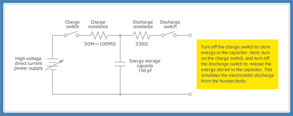
The human body model (HBM) is used as a method for testing the ESD in such interface terminals. This assumes that the electric charge which is charged inside the human body is discharged into the electronic device. Figure 1 is the human body model used in the electrostatic discharge immunity test according to IEC61000-4-2 standards.
Figure 1: Human body model for the electrostatic discharge immunity test (IEC61000-4-2)
Reasons why we recommend replacing a TVS diode with a chip varistor
Electronic components used for ESD/surge protection include MLCC (multilayer ceramic chip capacitors), ESD suppressors, TVS diodes (zener diodes), and chip varistors.
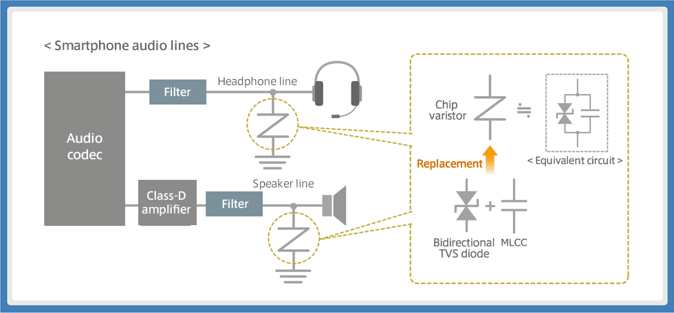
Figure 2 shows a circuit block diagram of the audio lines in a smartphone. In a smartphone, a Class-D amplifier, which is a digital amplifier, is used as the power amplifier for the speakers. And, the audio signals for the headphone line and microphone line are output directly from the audio codec. Therefore, protection components are inserted for ESD suppression in the speaker line and headphone line. There are several advantages in replacing a TVS diode, which is used as the aforementioned ESD protection component, with a chip varistor.
Figure 2: How to use ESD protection components in the audio line of a smartphone
While the ESD protection performance is almost the same for a TVS diode and chip varistor, there are various advantages in switching from a TVS diode to a chip varistor. While the major advantages are space saving and cost reduction, it is also effective in noise suppression. This is because a chip varistor has high capacitance, and also functions as an MLCC.
We shall first explain the space advantages of using a chip varistor which reduces the mounting area by a maximum of 90% or more.
Advantage 1. The mounting area can be reduced by a maximum of 90% or more
In recent years, there has been a rapid increase in the advanced functions offered by smartphones, and as a result, the main board has become extremely overcrowded, with no extra space. This has led to a trend towards using smaller electronic components than before.
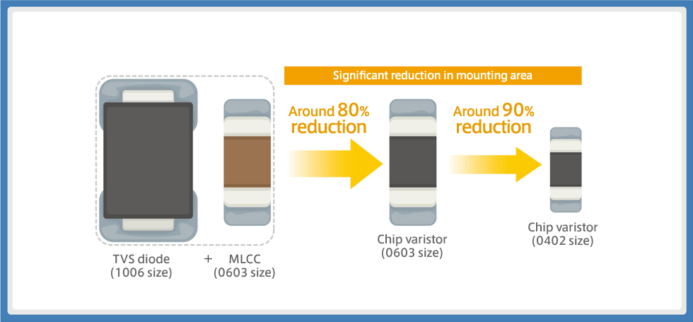
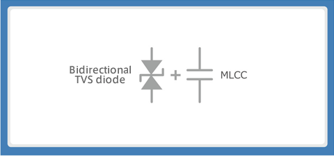
If the objective of audio line solutions using TVS diodes is ESD suppression as well as noise elimination, then, since a TVS diode has low capacitance, an MLCC needs to be inserted in parallel, therefore, the mounting area is required for the two components. However, since a chip varistor has high capacitance, two chips, namely, the TVS diode and the MLCC, can be replaced by a single chip.
Figure 3 shows a comparison of the mounting area when a TVS diode is combined with an MLCC and when a chip varistor is used. It is assumed that the component size is the 1006 size (1.0 x 0.6 mm) for the TVS diode, the 0603 (0.6 x 0.3 mm) size for the MLCC, and the 0603 size for the chip varistor. The mounting area can be reduced by 80% or more using the 0603 size of chip varistor, which is a tremendous saving of space. TDK also mass produces chip varistors in the 0402 size (0.4 x 0.2 mm), which reduce the mounting area by 90% or more, and can contribute to a further reduction in size and increase in functionality of smartphones.
Figure 3: Comparison of mounting area between a combination of two elements, a TVS diode + MLCC, and a single element, a chip varistor
Advantage 2. Low audio distortion
If you insert ESD protection components into the audio lines of a smartphone, it causes distortion of audio signals, leading to audio distortion. The extent of distortion is represented by value of THD+N (Total harmonic distortion + Noise).
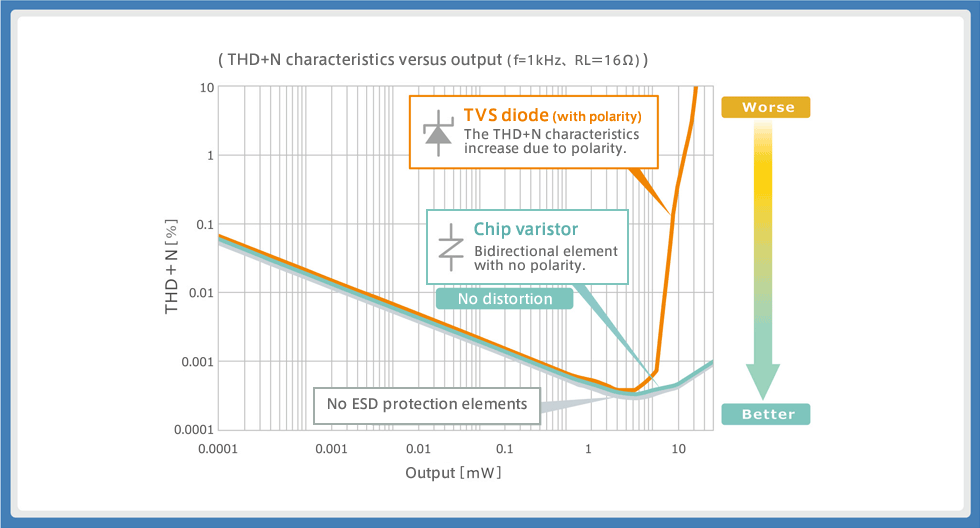
Figure 4 shows the THD+N characteristics versus output of ESD protection components. If you do not insert ESD protection components, the audio distortion is at its lowest, and this is the reference value. By inserting a TVS diode, there was a considerable increase in THD+N in the high output region. However, when a chip varistor was used, there was no audio distortion, similar to when no component was inserted.
Figure 4: Result of THD+N measurement for each ESD protection component
This shows the effect of the current - voltage characteristics (IV curve) of the TVS diode and chip varistor. The distortion in the audio signals appears to be generated because the IV curve of the TVS diode "rises sharply" and "sometimes has polarity".
Since the chip varistor does not have polarity, the characteristic of the IV curve is that it rises more gently than in case of the TVS diode. Hence, we can say that the chip varistor is more suitable than the TVS diode for suppressing the distortion in audio signals and maintaining high audio quality.
Advantage 3. Effect of noise suppression through capacitance
In the audio line of a smartphone, the noise generated by components such as the audio codec and Class-D amplifier interferes with the internal antenna and causes the reception sensitivity to deteriorate. To handle this, generally a low-pass filter (LC filter) is inserted, but, if possible, we would prefer to select the most suitable product from a wide range of capacitances.
Table 1 shows the capacitance range covered by various ESD protection components. It can be seen that the capacitance region covered by the MLCC is wide, ranging from a few pF to several µF, while that of the chip varistor ranges from a few pF to several 100pF, and that of a TVS diode ranges from a few pF to multiples of 10pF. The electromagnetic noise discharged from the wiring of audio lines is mainly in the frequency band ranging from a few 100MHz to several GHz, and to increase the noise attenuation effect in this frequency band, the use of a product with a capacitance ranging from a few pF to several 100pF is effective in noise suppression.
Table 1: Range of capacitance of various ESD protection components
The capacitance of TVS diodes with the 0603 size (0.6 x 0.3 mm) and the 1005 size (1.0 x 0.5 mm) is mainly in the range of 5 to 15pF, and to configure a low-pass filter to suit your requirements, you need to insert an MLCC in parallel with the TVS diode as shown in Figure 5. If you use only a TVS diode without an MLCC, the capacitance becomes insufficient to eliminate electromagnetic noise.
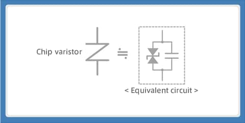
The available chip varistors with a capacitance ranging from several 10pF to several 100pF provide a noise suppression effect ranging from a few 100MHz to several GHz. As shown in Figure 6, the equivalent circuit of a chip varistor consists of a bidirectional diode and an MLCC arranged in parallel. TDK's chip varistors use a multilayer structure, and the capacitance can easily be adjusted by modifying the design of the internal structure. TDK offers a wide range of capacitances from the 1005 size (EIA0402): 650pF or less, to the 0603 size (EIA0201): 330pF or less, and you can select the product which matches the frequency band for which noise suppression is required.
Figure 5: Multilayer chip varistor equivalent circuit
Figure 6: Elimination of electromagnetic noise using TVS diodes
Advantage 4. Improved reception sensitivity
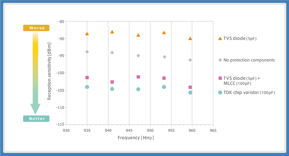
Figure 7 shows the result of measurement of reception sensitivity when ESD protection components are used.
When compared to the state where ESD protection components are removed (i.e. there are no protection components), a drop was observed in the reception sensitivity with the use of a TVS diode (capacitance: 5pF). When an MLCC (capacitance: 100pF) was inserted in parallel with this TVS diode, an improvement was observed in the reception sensitivity. On the other hand, an improvement in reception sensitivity was observed by using a single element when a chip varistor (capacitance: 100pF, AVRM0603C6R8NT101N) was used.
Figure 7: Result of measurement of smartphone reception sensitivity for each ESD protection component
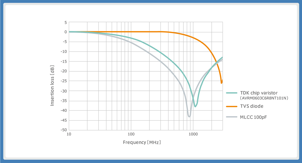
These results appear to be the effect of the transmission characteristics (insertion loss - frequency characteristics) corresponding to the capacitance of the ESD protection components. From the transmission characteristics of the ESD protection components in Figure 8, we can see that the chip varistor with capacitance of 100pF and the MLCC have the same characteristics, and the attenuation is large in the frequency around 1GHz. However, since the TVS diode has a low capacitance of 5pF, the attenuation region is around 3GHz, as a result of which it is not possible to improve reception sensitivity in the cellular band around 1GHz. To improve reception sensitivity in a solution using a TVS diode, it is necessary to insert an MLCC with a capacitance of 100pF in parallel.
Figure 8: Transmission characteristics of each ESD protection component (insertion loss - frequency characteristics)
Advantage 5. ESD protection effect
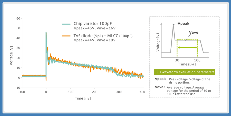
ESD protection is the basic performance characteristic of chip varistors and TVS diodes. In the electrostatic immunity test using the IEC61000-4-2 human body model (HBM), the ESD clamping waveform is used as the evaluation parameter, and the voltage of the rising portion is specified as the peak voltage (Vpeak), while the average voltage for the period of 30 to 100ns after the rise is specified as the average voltage (Vave).
Figure 9 is a graph which compares the ESD clamping waveform of the ESD protection components in the electrostatic discharge immunity test. It can be seen that the ESD protection performance of a TVS diode (5pF) is the same as that of a chip varistor when an MLCC (100pF) is connected to the TVS diode in parallel and inserted.
Figure 9: ESD clamping waveform of the ESD protection components
Summary of “Audio line solutions for smartphones using chip varistors”
TDK offers optimal solutions using chip varistors to suppress ESD in the audio lines of smartphones. Especially when replacing a TVS diode with a chip varistor, there are various advantages such as effective ESD suppression, space advantages, cost advantages, and noise suppression.
Advantages in replacing a TVS diode with a chip varistor
- Can achieve extremely good ESD protection.
- The functions of two chips, namely, the TVS diode (ESD protection) and MLCC (noise suppression) can be handled by a single chip of the chip varistor.
- Available in a wide range of capacitances, therefore you can select the product which matches the frequency band for which noise suppression is required.
- Can effectively attenuate the noise in the cellular band, and thereby improve reception sensitivity.
- THD+N, which is an index of audio distortion, is at the same level as when no components are inserted, and hence, audio quality can be ensured.
« Main features and applications of the chip varistor AVRM series »
[Main features]
- It is an SMD chip type of varistor which uses proprietary materials made of praseodymium based zinc oxide, and is manufactured using state-of-the-art multilayer processing technology and process technology.
- Since the current - voltage characteristics are symmetrical, there is no polarity.
- Though compact, it has excellent electrostatic absorption capacity.
- Available in a wide range of capacitances.
- In the audio lines of smartphones, you can switch from the TVS diode+MLCC to a single element.
- You can gain a variety of advantages by doing so, such as space saving, reduction in the number of components, reduction in mounting cost, etc.
[Main applications]
- ESD suppression in various electronic devices
(such as interface terminals, buttons/switches, battery terminals, etc.) - ESD suppression and noise suppression specific to the audio lines of smartphones
[AVRM series of chip varistors for audio line solutions] Product information and sample purchase
Recommended chip varistor products for the headphone line
| Application | Cap.(pF) | EIA0201 Part# | EIA01005 Part# |
|---|---|---|---|
| Headphone Circuit | 100 | AVRM0603C6R8NT101N | AVRM0402C6R8NT101N |
| 33 | AVR-M0603C120MTAAB | AVRM0402C120MT330N |
Recommended chip varistor products for the speaker line
| Application | Cap.(pF) | Over 2W(Vdc=17V) | 1W(Vdc=5.5V) |
|---|---|---|---|
| Speaker Circuit | 100 | AVRM1005C270KT101N | AVRM0603C120MT101N |
| 30 | AVR-M1005C270MTAAB | AVR-M0603C120MTAAB | |
| 15 | AVR-M1005C270MTABB | AVRM0603C120MT150N |
-
Related links
TDK also offers a variety of other solutions.
Please use them to build your products.
≫ Solution guide to the use of noise suppression filters in audio lines ≫ Solution Guide


