TDK TVS signal integrity for USB4® and Thunderbolt® 4 – protection of high-speed data lines and how to provide tailored ESD protectiontection

Contents
Electrostatic discharge and electrical phenomenon and protection
Peripheral devices using USB are widely used, and their connectors can be exposed to the environmental phenomenon of Electrostatic Discharge (ESD). This may lead to damage to sensitive electronic circuits within the portable devices. The standard approach to this problem is to add protection components inside, which suppress higher and potentially damaging voltage levels below the threshold levels of ICs by redirecting the over-currents away from the sensitive ICs and absorbing the energy delivered. These protection devices should be invisible to the circuitry during regular operation and should not impair the communication signal on the lines which are being protected.
Unlike USB 2.0 and the subsequent generations up to USB 3.2, which have been on the market for a long time and have been developed separately from other protocols, the USB4® and Thunderbolt 3 follow the same “USB4 Electrical Compliance Test Specification”. From a signal frequency point of view, Thunderbolt 3 signals and Thunderbolt 4 signals are the same. The ESD protection solution, therefore, is also the same. In practice, this means that ESD protection solutions designed for one of these protocols may be used for the other since the frequency used in the communication line is the same.
USB Type-C connector and TDK protection solution
The USB4 Implementers Forum (USB-IF) has worked on the latest protocol with the aim of offering display, data, and load/store functionality via a single USB4 Type-C® connector whilst also retaining compatibility with the existing USB ecosystem, including the compatibility with Thunderbolt® products via the USB4 Type-C connector, which also supports Thunderbolt 4 (TBT4) Systems in Alt mode [ref : www.usb.org]. This connector has been widely accepted due to the handy fact that it is invertible pluggable, which has been achieved by making mirroring pins on both sides of the connector. Those pins should be connected with adequate ESD protection since they can easily be exposed to an ESD event in everyday use.
The figure below shows the arrangement of the 24 pins used in the USB-C plug. The best practice is to place ESD protection as close as possible to the source of the transient event, i.e. to the connector. This means that miniaturized overvoltage suppressor devices are needed that do not take up much space and yet offer sufficient protection. Out of those 24 connector pins depicted below, four are used for ground connection and do not require protection. Receptacle interface [ref : www.usb.org]
USB Type-C receptacle interface (front view)
| A1 | A2 | A3 | A4 | A5 | A6 | A7 | A8 | A9 | A10 | A11 | A12 |
| GND | TX1+ | TX1- | VBUS | CC1 | D+ | D- | SBU1 | VBUS | RX2- | RX2+ | GND |
| GND | RX1+ | RX1- | VBUS | SBU2 | D- | D+ | CC2 | VBUS | TX2- | TX2+ | GND |
| B12 | B11 | B10 | B9 | B8 | B7 | B6 | B5 | B4 | B3 | B2 | B1 |
Due to the reversible design of the USB Type-C plug tip and the redundancy of the D+ and D- pins on the sides, 18 pins are connected. The D-/D+ are the pins used for connecting the USB 2.0 differential + and – pair. It is therefore sufficient if the receptacle side supports both USB 2.0 differential pair pins (placed above and in the below row), while the plug orientation determines which pair will be active.
GND – marked as Ground return, are all the ground return pins connected on the PCB.
Tx and Rx pins are used for high-speed data, and protection of such pins must be carefully chosen, considering the signal integrity on those lines.
VBUS – Bus Power pin, supporting higher voltages and currents, allows fast charging via those pins. Voltage rated on bus pins is up to 20 V and the currents up to 5 A, for a maximum power of 100 W.
USB full-featured Type-C plug (front view)
| A12 | A11 | A10 | A9 | A8 | A7 | A6 | A5 | A4 | A3 | A2 | A1 |
| GND | RX2+ | RX2- | VBUS | SBU1 | D- | D+ | CC | VBUS | TX1- | TX1+ | GND |
| GND | TX2+ | TX2- | VBUS | VCONN | SBU2 | VBUS | RX1- | RX1+ | GND | ||
| B1 | B2 | B3 | B4 | B5 | B6 | B7 | B8 | B9 | B10 | B11 | B12 |
In addition to the advantages of the USB Type-C port mentioned before, a USB PD (Power Delivery) protocol allows fast charging of end devices and more flexibility for the end user. The voltage specified for the USB PD is up to 48 V, and is available to use in combination with an Extended Power Range (EPR) cable [ref : “USB Type-C Cable Connector Specification,” October 2022] as shown below:
Summary of power supply options
| Mode of Operation | Voltage | Current | Notes |
|---|---|---|---|
| USB 2.0 | 5 V | See specification for USB 2.0 | |
| USB 3.2 | 5 V | See specification for USB 3.2 | |
| USB4 | 5 V | 1.5 A | See section 5.3. in the specification USB4 |
| USB BC 1.2 | 5 V | 1.5 A1 | Legacy charging |
| USB Type-C Current @ 1.5 A |
5 V | 1.5 A | Supports higher power devices |
| USB Type-C Current @ 3.0 A |
5 V | 3 A | Supports higher power devices |
| USB PD | Configurable up to 48 V |
Configurable up to 5 A |
Directional control and power level management |
Notes 1: Whereas USB BC 1.2 specification permits a power provider to be designed to support a level of power between 0.5 A and 1.5 A, the USB Type-C specification requires that a Source port that supports USB BC 1.2 be at a minimum capable of supplying 1.5 A and advertise USB Type-C Current @ 1.5 A in addition to supporting the USB BC 1.2 power provider termination.
CC – Configuration Channel pins and SBU – Sideband Use pins are used to detect connection configuration and for additional use of the Type-C connector for other protocols supported in Alternate (Alt) Mode, such as the HDMI protocol, for instance. [ref : USB.org]. Together with the VBUS and Differential (D+ and D- as shown above) pins, those pins are so-called low-speed signal line pins, while Tx/Rx pins are connected to high-speed communication lines.
This USB4 Type-C connector is also the connector of choice to become the “one for all” peripheral device connector for chargers in the European Union. With the new Radio Equipment Directive, the European Parliament enforces harmonization with charging ports and fast charging technology. After its adaptation by the European Parliament and the Council following ordinary legislative procedure (co-decision), there is a transition period of 24 months before becoming the standardized charger for EU countries. [ref : https://ec.europa.eu/commission/presscorner/detail/en/IP_21_4613 ]. Further standardization on USB and charging are found in the IEC 62680-1-2, Ed.5: 2021 "Universal serial bus interface for data and power Part 1-2: Common components - USB Power Delivery specification" and IEC 63002, Ed.2: 2021 "Interoperability specifications and communications method for external power supplies used with computing and consumer electronics devices"
TDK recently introduced TVS Transient Voltage Suppressor diodes are designed to fit the above application requirements. Protection of the high-speed Tx/Rx pins specifically requires carefully chosen ESD devices since this suppressor has to provide robust overvoltage protection for the ESD transients but also, during regular operation, it must not impair the signal on those lines. The data rates used for this signal go up to 20 Gb/s for USB4 20 Gbps and up to 40 Gb/s for USB4 40 Gbps, via two pairs. This means up to 10 Gb/s data rate for one line and up to 20 Gb/s data rate, respectively. The corresponding frequency for these data rates is roughly calculated by halving the data rate. Thus, this Nyquist frequency would be 10 GHz for the 40 Gbps data rate used with USB4, or 5 GHz for the slower 20 Gbps data rate, as shown in the table below.
USB data rate and frequency
| Total Data Rate | Data Rate / line | Frequency / line | |
|---|---|---|---|
| USB 3.2 Gen1 | 5Gbps | 5Gbps | 2.5GHz |
| USB 3.2 Gen2 | 10Gbps | 10Gbps | 5GHz |
| USB 3.2 Gen2x2 | 20Gbps (2 lines) | 10Gbps | 5GHz |
| USB 4 20G | 20Gbps (2 lines) | 10Gbps | 5GHz |
| USB 4 40G | 40Gbps (2 lines) | 20Gbps | 10GHz |
Signal integrity and protection approaches
An ESD component connected parallel to a data line inevitably entails some insertion loss, i.e. degradation of the signal quality. The degree to which the component affects the signal can be checked using eye diagrams for the corresponding signals. The best practice to ensure that the component will not degrade signals is to take measurements and assess. A test should be performed comparing eye diagrams of the signal tests recorded with a fixture with and without the component, using the standardized circuit. Two identical boards should be prepared, designed for working with HF signals. As shown in the figure below, one is populated with the ESD component, and one is without the component.
-
Reference boards without component

-
Reference board with component

The measurements with the same test signal should then be compared.
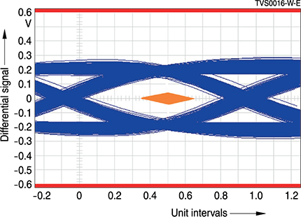
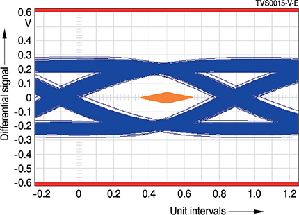
TDK ULC TVS diodes are tested using USB 3.2 signals, and the measurements are performed by the USB-accredited external lab, the Eurofins Digital Testing lab, which is certified for USB 3.2 signal tests and eye diagrams, with the respective signal mask provided below:
USB 3.2 Gen.2 eye diagram (10 Gbps per line, signal frequency 5GHz )
-
"With device" for TVS0016-W-E
-
"Without device" for TVS0015-V-E
Complete certified USB 3.2 Gen.2 compliance test report available upon request.
Tests are performed based on the worst-case scenario, which is the long channel test. The test is performed with a Standard-B receptacle, a cable length of 3 m, and additional PCB traces as per specification. A test based on selecting the worst channel for the host and the devices with Micro-B and Type-C products is also conducted. Both TDK TVS diodes from the ULC family have been tested and assessed as above and passed all tests. If a protection component passes the test with the USB 3.2 signals, this implies that those components will be a good choice for protecting lines with high data rate signals, with plenty of margin for other components needed on the line, but for lower data rates also.
TDK ULC TVS diodes are tested using USB4 signals as well. The same approach has been taken in those tests, and the eye diagrams are shown below.
20G Eye diagram
| 20.0G (Rounded) | |
|---|---|
| TP2_Pass through board 01005 | TP2_With TDK TVSD SDO1005 SL-ULC101 |
|
Eye Recovered - Delay by 3.133[pS] 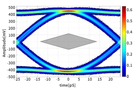 |
Eye Recovered - Delay by 3.133[pS] 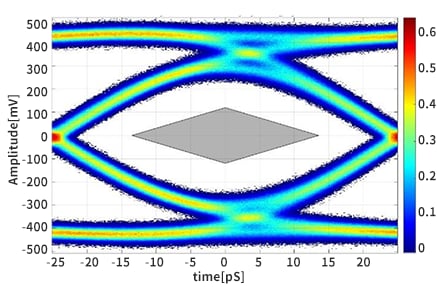 |
| TP3_Pass through board 01005 | TP3_With TDK TVSD SDO1005SL-ULC101 |
|
Eye Recovered - Delay by -0.392[pS] 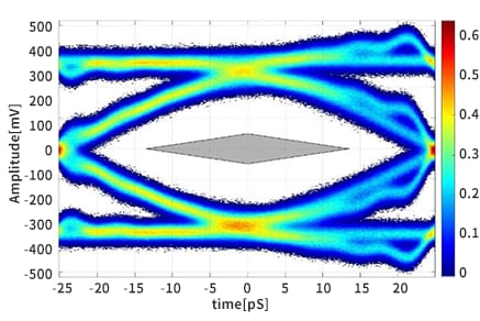 |
Eye Recovered - Delay by -1.762[pS] 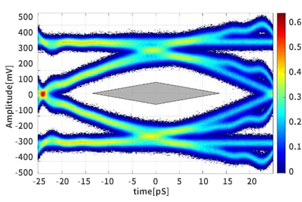 |
Where the points TP2 and TP3 are as specified in USB spec, as follows
USB4 TX compliance points definition

There is an embedded USB-C connector (simulated with S-parameters) and a passive cable (assumed length of the cable is for 10 Gbps 2 m and for rates of 20 Gbps is 0.8 m) between TP2 and TP3 points in the figure above [ref : www.usb.org].
Test signals used for the above tests and eye diagram measurements are nominal signals. While comparing those two measurements of the boards with and without components, only minimal differences can be observed, e.g., jitter values increased slightly. The test results show that TDK TVS ESD components have a clear pass with all tested signals.
TDK offers robust TVS ESD protection diodes compatible with USB 3.2 10 G and USB4 20 G and 40 G signals. Test reports for the USB 3.2 signals and USB4 for the referenced parts are available upon request.
TDK TVS ESD protection diodes compatible with USB 3.2 and USB4 40 G signals are available in two sizes with small volumes for applications with space constrains. The SD0201SL-ULC101 of size 0201 of EIA (Electronic Industries Alliance), the definition in “wafer-level chip scale” (WL-CSP) packaging
Transient Voltage Suppressors – TVS (SD0201SL-ULC101) and the SD01005SL-ULC101 of size 01005 acc. EIA in WL-CSP packaging Transient Voltage Suppressors – TVS (SD01005SL-ULC101) .
Both diodes consume very little PCB space, as given by the pad layout, and additionally their volume is also minimal, due to their thin package, with their height reduced to 100 µm. This is ideal for applications where there is not much space available. ESD protection is generally realized by placing the component in parallel to the protected circuit, and it may be placed anywhere on the line to protect the IC. The recommended approach is to connect them as close as possible to the source of disturbance placing the suppressor close to the connector. This way, the parasitic inductivities that may be generated are minimized. All components mounted behind the ESD components, as seen from the source of possible transients, are also protected. On top of this, by using leadless package any parasitic inductivities of the pins are also excluded. Therefore, SMD ESD protection device is very favorable for the described applications. The diodes operate quickly, and the advantages of the small package SMD WL-CSP package for ESD devices are apparent.
Looking at the signal path, there are many possible sources of insertion loss, which may introduce signal degradation. This includes chokes, CMCs, capacitors, cables, plugs, and connectors etc. Every part in the signal line will affect the signal in some way. The ESD component is an important part of this functionality, as it is essential to keep the IC safe from overvoltage transients. Looking at the figures showing eye diagrams for the worst-case scenario, the margin can be observed (marked with violet brackets below). This margin is what a developer has at their disposal to use for the components that will introduce additional insertion loss along the line, apart from the loss introduced by the ESD component already.
B74111U0033M060_TVS01005SL datasheet
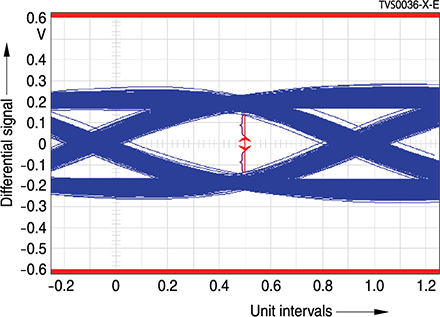
Since both the USB4 and Thunderbolt 4 follow the same "USB4 electrical compliance test spec", the test results are applicable for lines carrying Thunderbolt signal as well.
Product portfolio
The complete solution protection for the above explained pins of the USB Type-C connector is as follows.
| TDK Part No. | B74121U0033M060 | B74111U0033M060 | B74121U0055M060 | B74111U0055M060 | B74121G0160M060 | B74121G0200M060 |
|---|---|---|---|---|---|---|
| Footprint |  |
 |
 |
 |
 |
 |
| Package | WLCSP 0201 | WLCSP 01005 | WLCSP 0201 | WLCSP 01005 | WLCSP 0201 | WLCSP 0201 |
| Thickness | 150 μm | 100 μm | 150 μm | 100 μm | 150 μm | 150 μm |
| Working Voltage | 3.3 V | 3.3 V | 5.5 V | 5.5 V | 16 V | 20 V |
| Clamping Voltage ITLP = 8A | 3.9 V | 3.8 V | 4.1 V | 3.9 V | 22 V | 26 V |
| Capacitance 1 MHz | 0.65 pF | 0.48 pF | 0.55 pF | 0.43 pF | 9 pF | 5.3 pF |
| ESD level contact discharge | 15 kV | 15 kV | 15 kV | 15 kV | 15 kV | 10 kV |
| PIN to protect | Tx/Rx | Tx/Rx | D+/D-(Tx/Rx) | D+/D-(Tx/Rx) | VBUS (CCI SBU) | VBUS (CC / SBU) |
| Part No. lists |

Pins of the USB Type-C connector
The corresponding data sheets can be obtained following this link Transient Voltage Suppressors TVS – High-performance TVS Diodes for ICT, Consumer and High-speed Applications.
In conclusion, TDK TVS diodes offer state-of-the-art USB ESD protection, designed to provide excellent protection for sensitive IC and the tailored protection of the USB Type-C port pins and also for other applications. TDK TVS diodes occupy minimal space due to their miniature size and height, keeping a low clamping voltage level when protecting, without disturbing the signal of high data rates of, for instance, USB protocols and other high data rate protocols, as tested.
References
For more information on USB 4.0 specification, please check www.usb.org .
USB4®, USB Type-C® and USB-C® are registered trademarks of the USB Implementers Forum (USB-IF). Thunderbolt® is a registered trademark of Apple Inc..


