PCB Layout for ESD Countermeasures | ESD Visualization

Contents
- Introductory video (2:26)
- ESD Visualization System - Optimization of Board Layout -
- ESD behavior to difference in mounting location (Chip Varistor)
- Suitable mounting location of chip varistor for ESD countermeasures
- TDK chip varistor enables suitable ESD countermeasures & parts location
- Contact information
Introductory video (2:26)
ESD Visualization System - Optimization of Board Layout -
An ESD visualization system is a device that makes visible ESD current by automatically scanning the ESD flow with a non-contact magnetic field probe.
Since it can pick up the electric field intensity distribution in the scanning area, it is an effective tool for optimizing circuit board layout for ESD countermeasures.
By using this device, the behavior of ESD on a circuit board can be observed for board with different ESD protective element placements.
ESD behavior to difference in mounting location (Chip Varistor)
As shown below, Verification test was performed on the below PCB using an ESD visualization system.
The protection target is LED, and Chip Varistor is mounted below location.
Chip Varistor was mounted approximately 10 mm and 40 mm from the fulcrum in the figure below (★), and the ESD behavior was tested in each conditions.
Verification Conditions
- ◆ ESD applied voltage: + 1 kV
- ◆ Circuit Board: FR-4/Cu land pattern
- ◆ Land pattern: Pattern with multiple parallel mounting lines
- ◆ ESD protection parts: Chip Varistor (EIA0603, 27V, 430pF)
- ◆ Protection target: LED (ESD withstanding voltage: 6 kV)
- ◆ Mounting location: Approximately 10 mm and 40 mm (indicated by ★ in this figure)
This shows the ESD behavior with Chip Varistor mounted approximately 10 mm (left) and 40 mm (right) away.
It can be seen that with Chip Varistor located closer, the ESD passes to Chip Varistor does not pass on the LED line.
[Mounting location: 10mm]
[Mounting location: 40mm]
It can also be seen that when Chip Varistor is mounted approximately 10 mm position, the ESD passes to Chip Varistor side immediately after entering the circuit, and at the peak, ESD path is dominated at Chip Varistor side.
Time Lapse Before & After ESD (Mounting Location: 10mm)
On the other hand, when Chip Varistor is mounted approximately 40 mm position, the ESD passes to the LED line immediately after entering the circuit, and at the peak too, ESD passes to the LED line.
It shows that the LED is applied high electrical load by ESD.
Time Lapse Before & After ESD (Mounting Location: 40mm)
Suitable mounting layout of chip varistor for ESD countermeasures
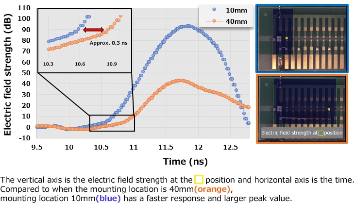
In the analysis of the electrical field strength, Chip Varistor 10 mm position (indicated in blue) responds about 0.3 ns faster than 40mm conditions.
In generally, ESD rise time is about 1 ns. therefore this 0.3 ns time makes a substantial difference.
In addition, for ESD response time is faster, the electric field strength is also high at the peak.
In other words, Chip Varistor mounted closer to the ESD intrusion point can respond faster and more the ESD.
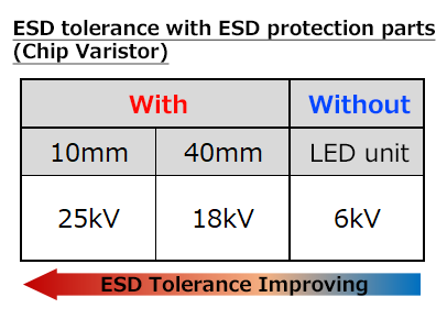
When actual LED's ESD tolerance was tested under the verification conditions indicated above, It was found that the ESD tolerance was improved by using chip varistor and parts layout closer to the ESD intrusion point.
For better ESD countermeasures, chip varistor mounting layout is key element. Chip varistor is best to be close to the ESD intrusion point.
ESD Test Conditions
- ◆ Test Standard: IEC61000-4-2 (150pF/330Ω)
- ◆ Direction: Bi-direction
- ◆ Number of Discharge: Each 10times
TDK chip varistor enables suitable ESD countermeasures & parts location
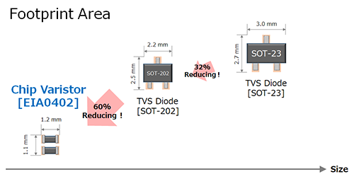
In conjunction with the increasing complexity of circuit boards, even if ESD intrusion point are identified, nearby mounting space may be limited.
One of the features of TDK Chip Varistors is wider case size lineup including small package type.
TDK currently supports mass-production of Chip Varistors with minimum size of EIA01005 (0.4 x 0.2 mm) for consumer grade and EIA0402 (1.0 x 0.5 mm) for automotive grade.
Therefore, by using TDK Chip Varistor, space saving and mounting with high degree of freedom is possible.


