Preventing Flex Cracks in MLCCs: How Solder Land Dimensions and Circuit Wiring Patterns Contribute towards Stress to MLCCs
 Contact Us

What Are MLCC Flex Cracks? Mechanism and Impact
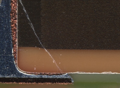
Flex cracks in MLCCs caused by substrate bending stress
A flex crack is a phenomenon in which mechanical stress from board bending is applied to an MLCC soldered onto a PCB, causing a crack in the ceramic body. Ceramics are resistant against compression but weak against tension. Excessive tensile stress from board bending can therefore cause cracks in the body of MLCC.
- If a crack penetrates the area where the internal electrodes overlap, it may lead to reduced insulation resistance or a short circuit.
- Crack patterns vary with the board's deformation state and mounting conditions. Cracks may be observed in various shapes, such as Y-shaped or slanted.
- In general, a crack is considered to occur when the stress caused by board deformation exceeds the strength of the ceramic body. Countermeasures from the design stage are crucial for applications that require high reliability.
When Flex Cracks Occur
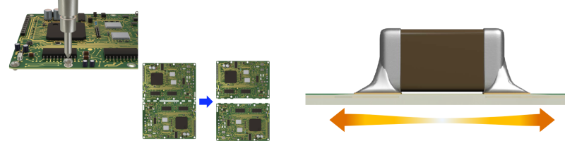
After an MLCC has been soldered to a PCB, any operation that significantly bends the board can be a risk that causes flex cracks. Typical examples include the following:
- PCB cutting
- Connector installation
- Wiring harness installation
- Screw fastening
- Board handling
- Drops and impacts
In addition, the magnitude of the stress applied to the MLCC changes with the bending direction of the board and the placement of the MLCC.
Basic Measures to Prevent Flex Cracks
To prevent flex cracks, it is important to avoid applying unnecessary external force to the board. Effective measures include installing board reinforcements or supports, checking manufacturing processes, checking board depanelization conditions, and reviewing component placement.
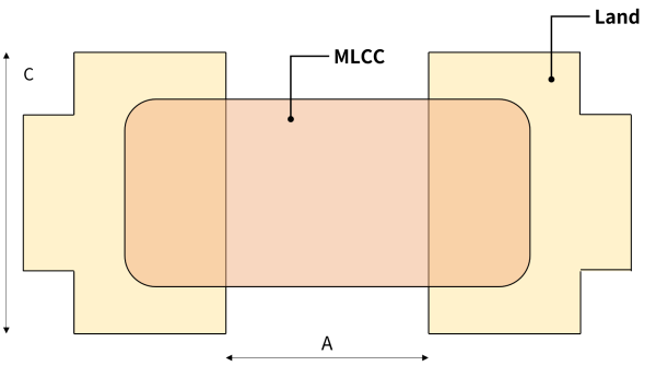
The solder land's dimensions and shape and wiring patterns are also among the factors that influence the stress applied to an MLCC. This article presents how the stress around the MLCC changes when the solder land's A and C dimensions and the circuit trace extending from the MLCC's end side are modified.
Effect of Solder Land Dimensions and Wiring Patterns on Stress [Analysis Results]
1. Positional Relationship Between Solder Land and MLCC
TDK focused on three factors in the solder land-MLCC positional relationship shown in Figure 1: the A dimension, the C dimension, and the circuit trace extending from the MLCC's end side. TDK analyzed the stress distribution before and after changing each factor. The results are shown on the table below. The effectiveness differs by factor.
| Design factor | Change | Stress reduction in analysis |
|---|---|---|
| A dimension (land length between electrodes) | Shorten | Reduced, but the reduction is relatively small |
| C dimension (land width) | Shorten | Reduced, but the reduction is relatively small |
| Circuit trace on MLCC's end side | Reduce | Relatively large reduction (most effective) |
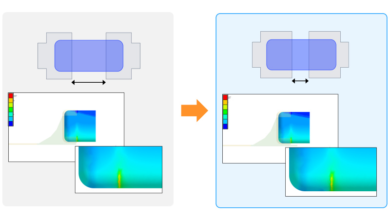
2. Effect of the A dimension
Shortening the A dimension reduced the stress around the MLCC by approximately 12%.
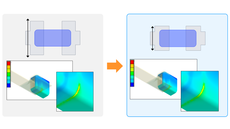
3. Effect of the C dimension
Shortening the C dimension also reduced the stress around the MLCC, by approximately 10%. This reduction rate is almost the same as for the A dimension. It shows that the effect of this factor alone is limited.
4. Effect of the circuit trace extending from the MLCC's end side
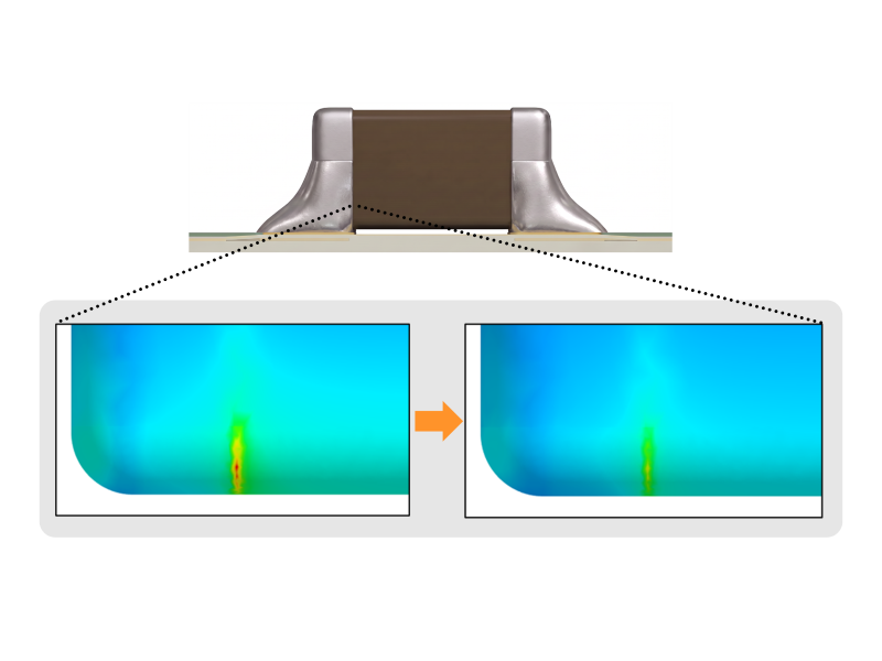
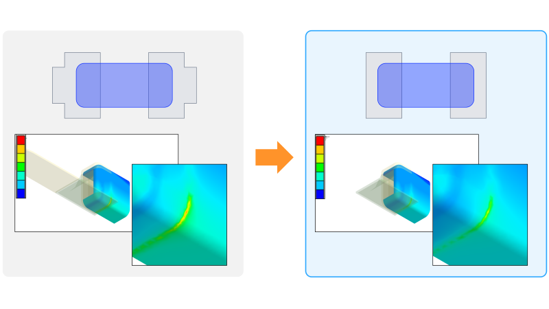
In contrast, reducing the circuit trace extending from the MLCC's end side lowered the stress by approximately 26%, showing significant improvement in comparison with changing the A or C dimension.
The stress distribution before and after improvement is shown in Figure 5.
| Design factor | Stress reduction (approx.) | Effectiveness |
|---|---|---|
| Shortening the A dimension | 12% | Small |
| Shortening the C dimension | 10% | Small (almost the same level as A) |
| Reducing circuit trace on end side | 26% | Large (most effective) |
Shortening the A or C dimensions therefore gives a similar, limited stress reduction. Reducing the circuit trace extending from the MLCC's end side showed a significantly larger effect than the other two factors. When reviewing solder land design, it is considered effective to examine the wiring pattern first.

Note: Reduction rates are calculated relative to the terminal stress before any changes.
5. Design key points
Rather than relying only on adjusting the solder land dimensions (A and C), giving priority to reducing the circuit trace extending from the MLCC's end side is considered effective for lowering stress.
*Note: This analysis is a comparison under specific conditions using simulation (1/4 symmetrical model). It does not guarantee performance in actual equipment or product reliability.
FAQ
Q1. Which of the three factors should I review first?
A. In TDK's analysis, reducing the circuit trace extending from the MLCC's end side lowered stress the most. The effects of shortening the A and C dimensions are relatively small. It is therefore considered effective to examine the circuit trace first.
Q2. Are adjustments to the A and C dimensions ineffective?
A. They are not ineffective; shortening them does reduce stress. However, under TDK's analysis conditions, the reduction was relatively small. We recommend combining with other countermeasures.
Q3. Can solder land design alone prevent flex cracks?
A. Solder land design is one of the contributing factors. Based on assumption that a combination of countermeasures is executed, including board reinforcement, process control, board depanelization conditions, and a review of component placement, verification by testing on actual equipment is essential.
Conclusion | Improve Reliability with Combined Countermeasures, Centered on Reducing the Wiring Pattern
For MLCC flex crack prevention, shortening the solder land's A and C dimensions also contributes to lower stress. In TDK's analysis, however, reducing the circuit trace extending from the MLCC's end side was the most effective. In design, reviewing the circuit trace is an effective core method. Combination with optimization of component placement, board depanelization conditions, and process control is effective.
TDK supports designers' decisions by analysis & visualization of the change in stress distribution before and after improvement, with focus on the A and C dimensions and the circuit trace on MLCC's end side. For more analysis examples and high-reliability MLCC series, see the TDK Tech Library solution guide "Flex Crack Countermeasures in MLCCs." Early-stage design review contributes to improving the overall reliability of the final product.
Related links:


Related Links